5305

ECEA 5360 - Introduction to FPGA Design for Embedded Systems


Course description

Course books: FPGA for Dummies


  1. An FPGA is an integrated circuit designed to be configured by a customer or designer after manufacturing. The design is dictated by a Hardware Design Language (HDL) like Verilog or VHDL.
  2. Books for the course: Rapid Prototyping of Digital Systems: SOPC Edition, by Hamblen, Hall and Furman; ISBN 9780387726700 and Design Recipes for FPGAs Using Verilog and VHDL, 2nd Edition, by Peter Wilson
  3. XC2064 - The First FPGA
  4. Digital Logic encompasses Standard Logic (TTL/CMOS devices), Programmable Logic (FPGA's PLDs, CPLDs), ASICS, and Full Custome (Microprocessor & RAM). Standard Logic Integrated Circuits include all of the previous except ASICs.
  5. FPGA's consist of: a wire, a gate, and a register/flip-flop. The chips has these three in arrays to create complex logic patterns.
  6. An ASSP (Application Specific Standard Product) is built to order for a general purpose market. ASIC's are built for one specific purpose
  7. System on Chip (SoC) - Integrated Circuit that integrates all parts of a computer onto a single chip. Or integrating more than one componnent along with a CPU onto a single chip.
  8. If FPGA is included on an SOC it is an Programmable SoC or an FPGA SoC.
  9. CPLD = Complex Programmable Logic Device, have a different arch than FPGA's. Use a PAL, some of the more complex ones would tie these PAL's (programmable AND, fixed OR) into larger "macrocells", which could be fed into each other. Lots of initial CPLD's were used this way as a chip select.
  10. CPLD's timing is very predictable (deterministic in the slides, this seems like a stretch to me). They have super wide inputs, probably why they're used for chip selects.
  11. Bad for many registers, data transfers, bus transfers
  12. FPGA's were first designed to imitate gate arrays. The logic is instead implemented with Lookup Tables (LUT)
  13. FPGA logic element is usually implemented as a LUT. An FPGA (simple version) consists of a 4 input LUT, Full Adder (FA) and a D Type Flip . Wide inputs can be created by cascading these logic cells, which can cause excessibe delays compared to a CPLD for a similar wide input.
  14. HDL Languages, moving from EEPROM to RAM, and moving beyond just boolean
  15. FLASH FPGAs are very reliable and reprogrammable, and have better security since they can only be programmed once, and are hard to reverse engineer because of a security fuse. Antifuse are not reprogrammable and SRAM are not suitable for high reliability.
  16. CPLD's can be less expensive and can meet very tight and deterministic timing constraints.
  17. Full bit adder can be constucted in as little as 5 gates. RTL = register transfer logic
  18. Can connect full bit adders by carry them togeter (ripple bit adder). this is rather slow total delay:
  19. Carry look ahead adder is a faster way to make an adder.
  20. In an FPGA we can use LUTS to use ripple bit array, but with fewer gates.
  21. Multipliers are common digital logic functions, but have historically been difficult to make.
  22. Can make array multipliers but the gates increase by n^2, which quickly makes sequential circuits more practical past 4 bit x 4 bit multipliers.
  23. To build in an FPGA 1. Combination circuits (fast and big), 2. sequential shift and add (state machine), specialty algorithms (complex), memories (doesn't scale well), 5. Some combo of above, 6. Hard multiply blocks.
  24. A 4x4 mult can be achieved with a memory with an 8 bit address. Beyond 8x8 bits. it becomes impractical
  25. Hard multipliers provide the greatest speed of any FPGA implemnation

Actually using Quartus

  1. Design Entry (schematic/HDL) -> functional simluation -> synthesis or mapping -> Place and route/fitting -> Simulation - > Programming -> Test and Integration
  2. FPGA design steps include Test and Integration, Functional Simulation, and Programming. This is Analysis & Synthesis, fitter, assember, timing analysis, eda netlist writer in your the design flow window within quartus.
  3. You can enter designs via AHDL Files, Block diagram/schematic file, EDIF file, Qsys System file, state machine file, systemverilog hdl file, tcl script file, verilog hdl file, and VHDL file.
  4. Quartus for linux seems to be working better than I expected. This course expects a super old version (v16), but I ended up having to run 18.1 to reliably work on my Debian 12 machine. I also had to do this insane hack to get the X windows to not fail on me. It was just hanging with "mega_lpm_muxq" at 100% CPU usage. There has got to be a way to configure X to fix this as well. ssh -Y localhost fullpathtoquartus works though.
  5. IP Cores are pre-made design blocks which can be customized in Quartus Prime.
  6. The Quartus Prime Compiler is a set of software modules that performs synthesis, fitting, assembly, and analysis, generates programming output files, runs modules together or independently, optimizes results through compiler settings, and generates reports for analysis.
  7. Quartus order of compilation: Analysis and Synthesis -> Fitter [Place and Route] -> Assembler -> TimeQuest Timing Analysis -> EDA Netlist Writer
  8. The Power Play Power Analyzer provides postfit power estimations. Not the most accurate, but useful for making design decisions.
  9. Fmax (fastest the clock can go) is a critical measurement for FPGA design.
  10. Positive slack indicates timing closure whereas negative slack indicates setup or hold violations (i.e. it is going over time).
  11. RTL Viewer allows viewing the design from the simplest perspective, just the logic! Used for verifying design entry/logic. Available after analysis.
  12. Try to use the compiler to make changes you want! Chip planner is better for analysis, the compilation algorithms are complicated.
  13. Darker color = chip is used more in a design within the chip planner
  14. Use the chip planner to: Create a design floor-plan, Implement Engineering Change Orders (like moving a pin), view device resourecs laid out on the device, find timing issues, and examine fan-in and fan-out of specific device resources.

Timing Analysis Fundamentals

  1. Data must be stable before and after the clock edge to be reliably transferred. If not properly synchrnozed there could be hazards (unexpected or undesired signals), metastability - a condition caused by timing vioaltions and flip-flop outputs leading to erroneous data, race conditions bugs that come and go, clock skew
  2. Static hazards occur as the consequence of unequal delays in logic. One way to remove the hazard is to add another gate. The best way is to use flip-flops with synchronous design!
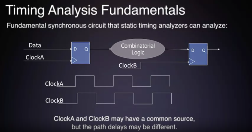
  3. Clock A and Clock B may have the same source, but may have different delays.
  4.          Launch Edge = Clock Edge that activate sthe source register in a register-to-register path.
             Latch Edge = Clock edge that activates the destination register and captures the data. Together they form a data requirement window.
             
  5.          Data Arrival Time = the time for data to arrive at a destination register's D input from the common clock edge.
             Data (Setup) Arrival Time = Launch Edge + TclkA + Tco + Tdata
             
  6. Clock Arrival Time = the time for clock to arrive at a destination register's clock input
  7. Hold Time is defined as the minimum time the data signal must be stable after the clock edge
  8.          Data Required Time = the minimum time for the data to get latched into the destination register (AFTER the hold)
             Data Required Time Hold = Clock Arrival Time + Th
             Typical value is around 1 ns
             
  9.          Data Required Time (Setup) = the minimum time required for the data to get latched into the destination register (BEFORE the hold)
             Data Required Time (Setup) = Clock Arrival time - Tsu (setup time usually specified in FPGA)
             
  10.          Setup slack = the margin by which the setup timing requirement is met
             Setup Slack = Data Required Time (Setup) - Data Arrival Time
             Setup Slack = Clock Period + TclkB - Tsu - TclkA - Tco - Tdata
             
  11.          Hold Slack = The margin by which the hold timing requirement is met
             Hold Slack = Data Arrival Time - Data Required Time (Hold)
             Hold Slack = TclkA + Tco + Tdata - TclkB - Th
             
  12. When all timing is met, time enclosure is occuring. This is often a main goal of an FPGA's design.
  13. I/O timing analysis uses the same slack equations.
  14. Need to understand these to undersatnd cause of violation. Example causes, data path too long, requirements too short (incorrect analysis), large clock skew signifying a gated clock etc
  15. How to use timing quest analysis
    1. Generate Timing netlist
    2. Enter SDC constaints (Create and/or read in SDC file), constrain directly in console
    3. Update timing netlist
    4. Generate timing reports
    5. Save timing constraints
  16. User MUST enter constraints for all paths to fully analyze design. Timing analysis only performs slack analysis on constrained signals. Constraints guide the fitter to place & route design in order to meet timing requirements. Prof recommends constraining all paths! (or at least clocks & I/O)

Timing within quartus!

  1. Using Timequest Timing Analyzer (it's now just called Timing Analyzer)
  2. The Timing Netlist is composed of the names of all source and destination timing elements in the design, as well as minimum and maximum timing path relaying information. Derives this from timing results.
  3. Cell - basic device building blocks (LUTs, registers, multipliers, memory, PLLs) Pin - input or output of a cell Net - connections between pins port - top level device pin
  4. The input delay is the net sum of all external delays, typically consisting of the delay from the common clock source, to the external device flip flop plus the flip flop clock to out delay, plus the delay in the PCB traces to the FPGA input, minus the delay from the common clock source to the FPGA clock input. To be accurate, you'll need measurements or models of the PCB delay, and data sheet information for the external device that drives the inputs.
  5. Register Transfer Level Simulation, Gate Level Timing Simulation, and Gate Level Functional Simulation are supported by Quartus Prime.
  6. Altera Modelsim wouldn't run. Following this forum post Had to chmod u+w vco so I could write it.
  7. Uses this SO to get more libs: https://askubuntu.com/questions/1121815/how-do-i-run-mentor-modelsim-questa-in-ubuntu-18-04
  8. This guy is the realest one! https://blog.bachi.net/?p=8523 https://download.savannah.gnu.org/releases/freetype/freetype-old/
  9. Had to manually include lpm_ver library via vsim -L lpm_ver

Different types of FPGA's

  1. Criteria for selecting a FPGA
  2. Provide ample amounts of logic - measured by system gates, logic elements, slices, macrocells, LABs, ALMs, etc.
  3. Cost per gate is also important
  4. Speed - measured by maximum clock frequency (Fmax)
  5. Low power consumption - varies from microwatts to hunderds of watts. This is often in opposition with speed. Static power is how much the FPGA consumes while doing nothing.
  6. Repgrammabiltiy - dependent on configuration, makes it easier to develop/deploy if you can program more than once.
  7. Amount and type of I/O - thought in terms of cost per I/O and I/O density.
  8. Inclusion of Hard IP cores, like those for Memory, DSP blocks, transcivers and hard processors
  9. CPLD's ans smaller FPGA's are structured so that timing is more deterministic
  10. Reliability, measured by FIT rate or MTBF
  11. Endurance of configuration memory - issue for long lifetime
  12. Design and data security.
  13. 11 categories for this course: Repgrammability, Size/Logic Density, Cost Per Logic Gate, Speed (FMax), OPower consumtion, cost per i/o relative to i/o density, Hard IP available on chip, deterministic timing, reliability (FIT rate), Endurance (number of programming cycles and years of retention), design/data security
  14. When creating a pipeline by inserting flip-flops to break up long combinational delays, the clock can now run faster, but the data will have more latency as it moves through the pipeline.
  15. Most common sources of FPGA failures or delays: #1 Timing Closure, #2 High Speed Interfaces (PCIe, DDR3), #3 Pin assignments and I/O errors
  16. I/O standards vary greatly, even within one FPGA. I/O is organized in banks with one voltage reference +3.3, +2.5 and +1.8 are common. One bank may be different from the next. Single ended I/O are LVTTL or LVCMOS with many variations including HTL, SSTL, GTL etc.
  17. Differential I/O typically LVDS but also LVPECL, CML, etc.
  18. Global nets are usually assigned to specific pins that can also be I/O. Board layout must use these pins as clocks or reset if global nets are to be used.
  19. In altera FPGA's, you can do pin assignment in one of 5 ways 1. Using quartus gui tools, either the pin planner or assignment editor 2. Importing from an sdc file or excel spreadsheet file 3. Writing directives in an HDL (Verilog or VHDL) file 4. Automating by use of a TCL script, 5. Importing from a PCB layout CAD Tool